KiCad Tutorial 2026: Design Schematics, Build PCBs, and Generate Gerber Files Like a Pro
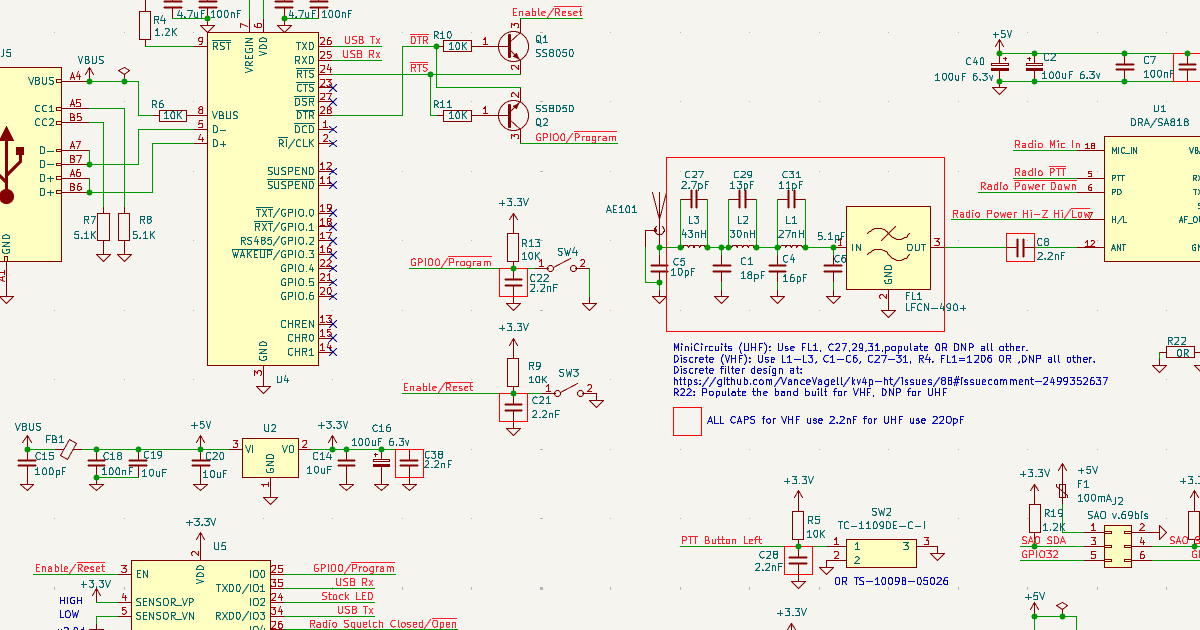
KiCad Tutorial 2026: Design Schematics, Build PCBs, and Generate Gerber Files Like a Pro
KiCad Circuit Design Software Usage Guide
Part 1: Schematic Design
1.1 Create a New Project
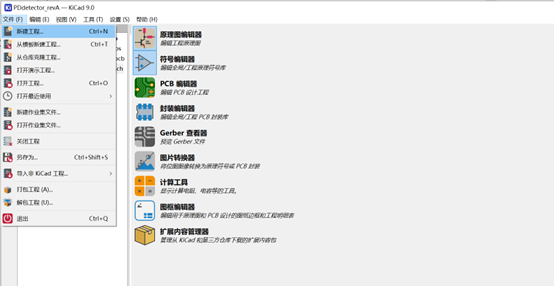
1.2 Open Schematic Design
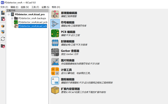
1.3 Double-click to Open the Schematic
By default, this opens the root schematic page. 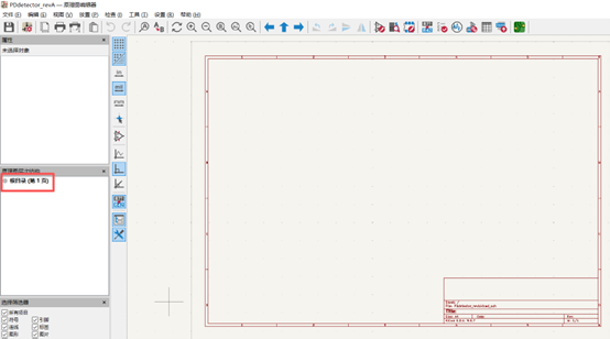
1.4 Use Hierarchical Schematic Structure
The root directory mainly defines the overall logical relationships. 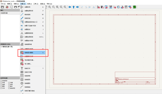
1.5 Create Hierarchical Schematics
Assign meaningful names to hierarchical schematic sheets. 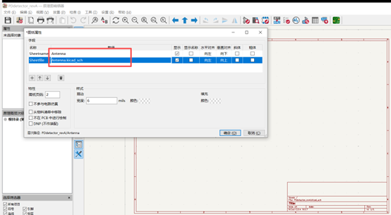
1.6 Enter Specific Sheets
Select components and begin drawing the schematic. 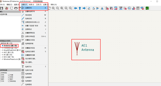
1.7 Configure Display Settings
Adjust page view, cursor, and display preferences. 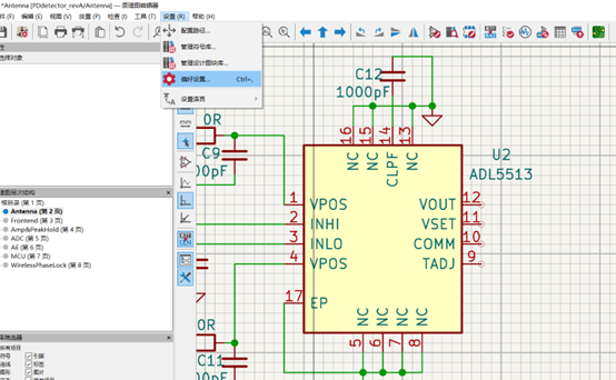
1.8 Draw Schematic Symbols
Use and modify existing symbols as needed. 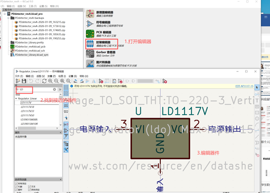
1.9 Create a Schematic Library
Manage custom schematic symbols efficiently. 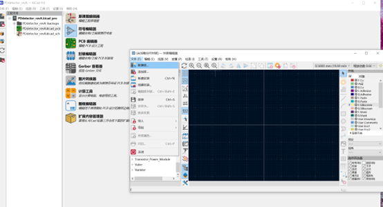
1.10 Save Symbols to Your Library
Store completed symbols in your custom library for reuse. 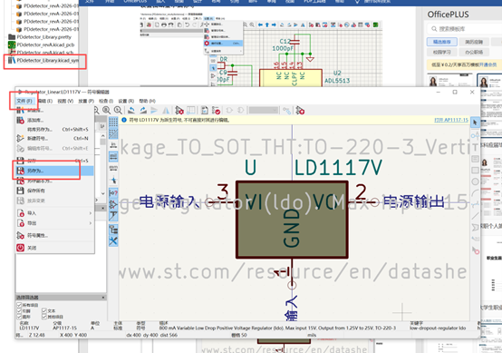
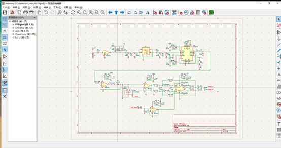
1.11 Complete the Schematic Framework
Part 2: Schematic Refinement and Adjustment
2.1 Assign Reference Designators by Page Number
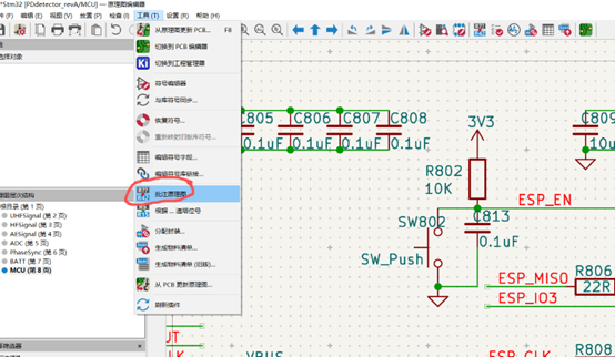
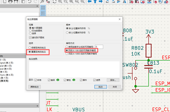
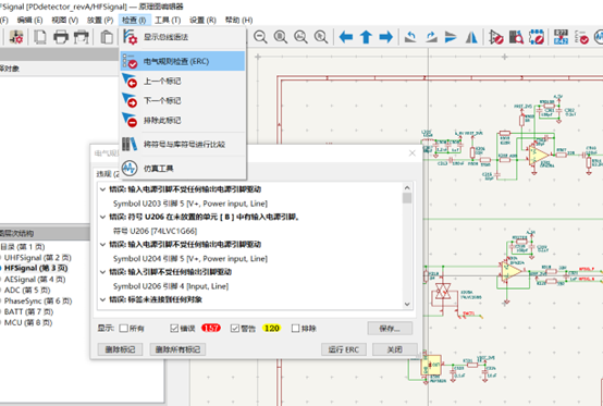
2.2 Run DRC (Design Rule Check)
2.3 Use Net Labels in Schematics
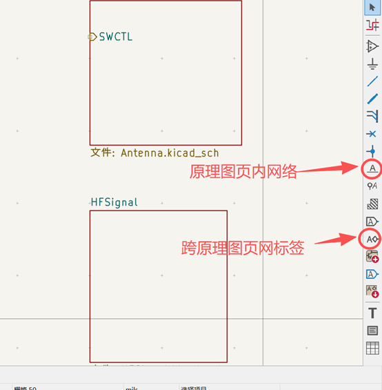
2.3.1 Place Hierarchical Labels Across Different Sheets
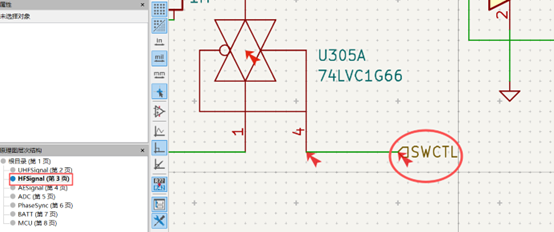
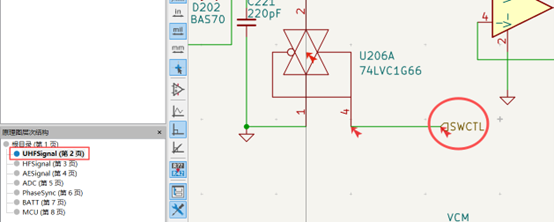
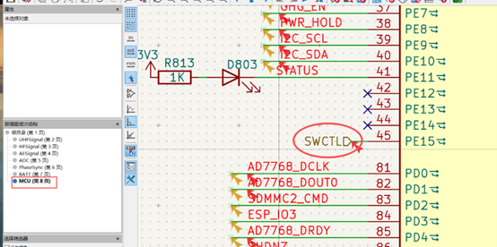
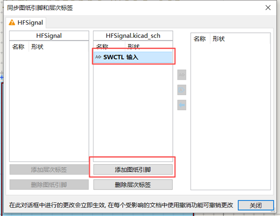
2.3.2 Synchronize Pins and Labels in Root Sheet,Connect hierarchical labels properly.
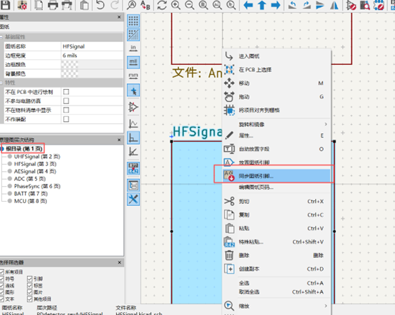
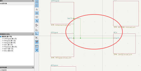
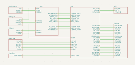
2.3.3 Connect All Hierarchical Labels in Root Sheet
2.4 Edit Symbol Properties
2.4.1 Modify Symbol Attributes,Adjust properties based on requirements.
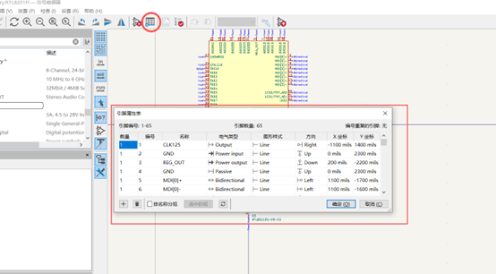
2.4.2 Update Library and Synchronize Changes
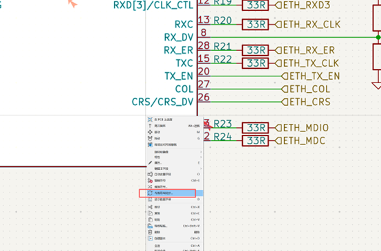
Part 3: Preparation Before Importing to PCB
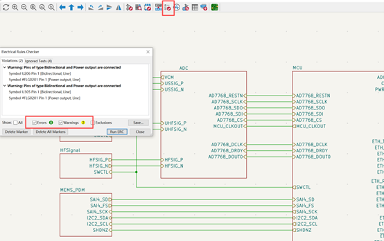
3.1 Perform DRC Check, Ensure no errors; review warnings for PCB impact.
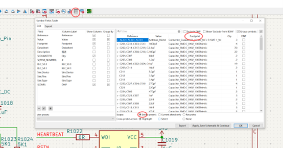
3.2 Assign PCB Footprints to Symbols
- Verify page by page
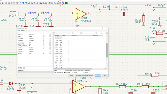
- Select footprints from libraries
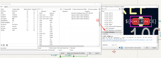
- Modify individual symbol footprints if needed
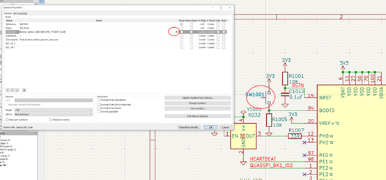
- Ensure all symbols have correct footprints
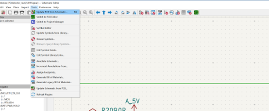
3.3 Import Symbols and Connectivity into PCB
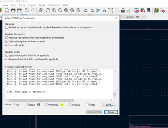
3.4 Import Components into PCB
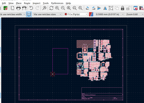
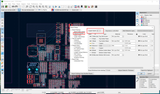
3.5 Configure PCB Layer Stack
Part 4: Useful Tools in PCB Design
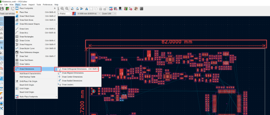
4.1 Add Dimension Annotations
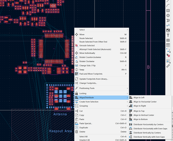
4.2 Align Components
4.3 Chamfer Board Outline
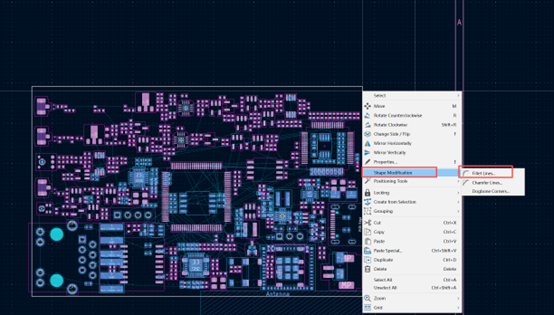
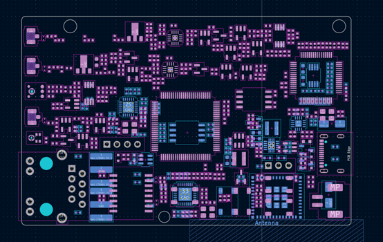
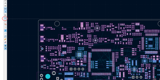
4.4 Show/Hide Net Connections
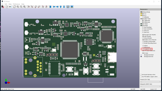
4.5 Hide Reference Designators in 3D View
4.6 Define Routing Rules
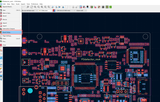
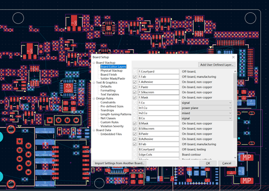
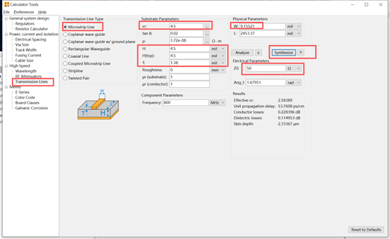
4.7 Set 50 Ohm Impedance Traces
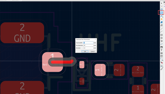
4.8 Adjust Trace Width During Routing,Shortcut key: “E”
4.9 Hide Specific Net Ratsnest Lines
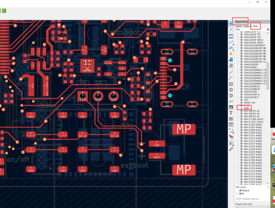
4.10 Highlight Nets
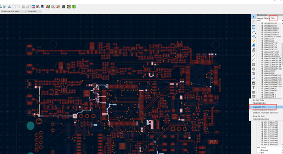
4.11 Hide Silkscreen Reference Designators
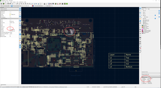
4.12 Length Matching Routing,Use the length tuning tool.
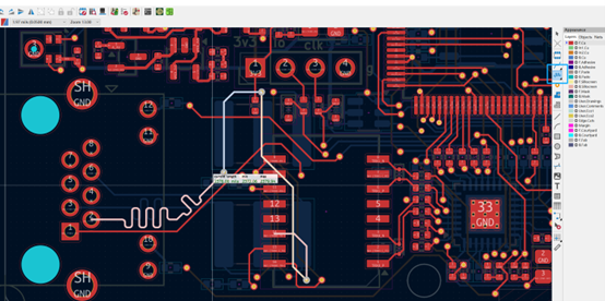
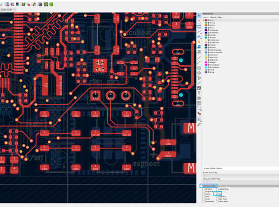
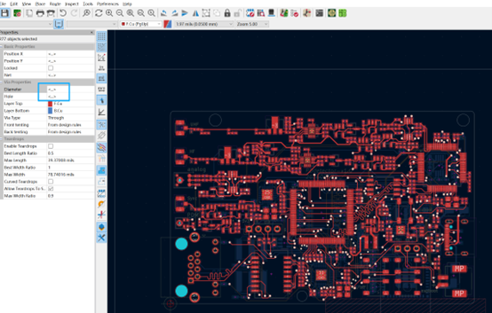
4.13 Batch Modify Via Sizes
- Select the region
- Modify via parameters
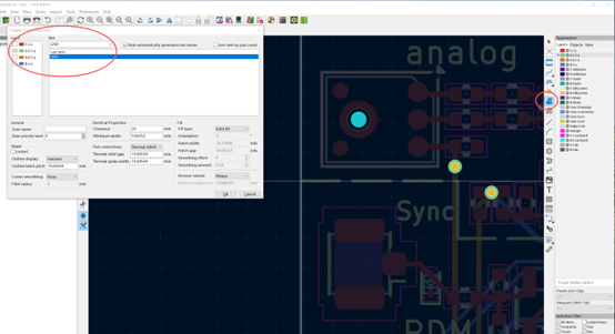
4.14 Set Copper Pour Nets
Part 5: Generate PCB Manufacturing Data
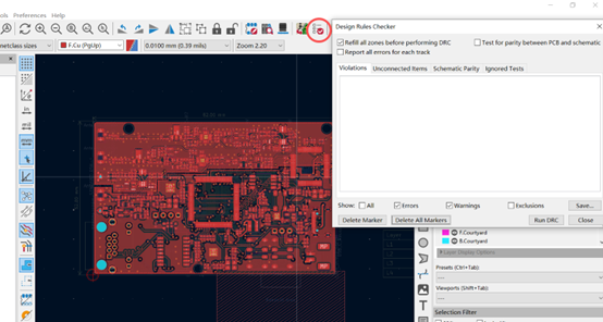
5.1 Perform Final DRC Check
5.2 Generate Gerber Files
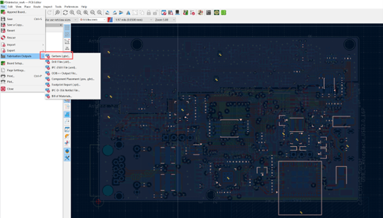
Select file save location. 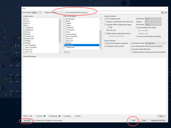
5.3 Generate Drill Files
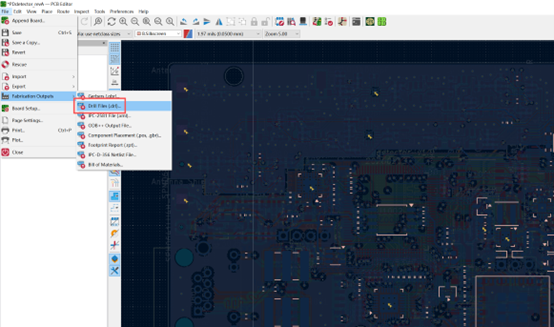
Save in the same location as Gerber files.
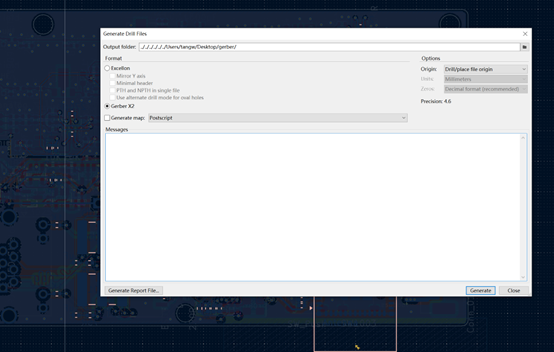
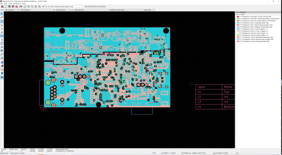
5.4 Use KiCad Gerber Viewer Verify generated files.
5.5 Generate Position (Pick-and-Place) Files
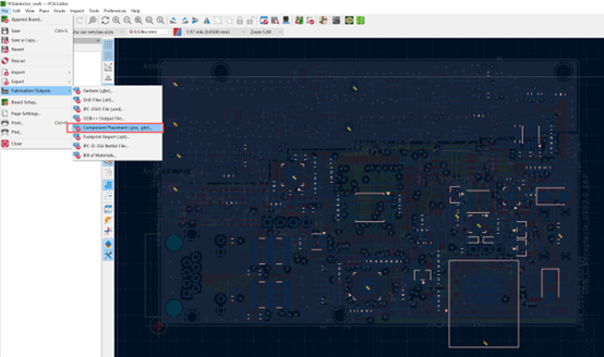
Choose save path. 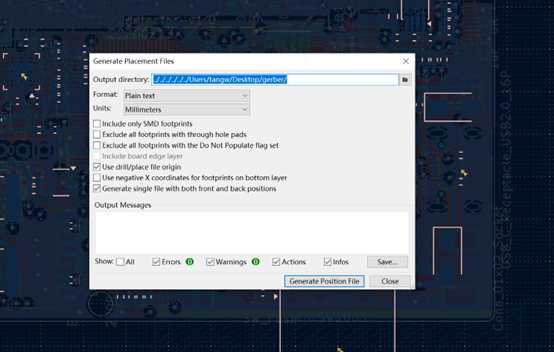
5.6 Generate BOM (Bill of Materials)
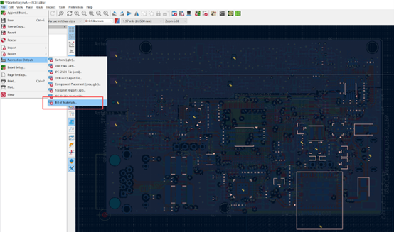
OK, all done!
This post is licensed under CC BY 4.0 by the author.