LoRa Flood Sensor Development Series - Part 3 PCB Placement Guide
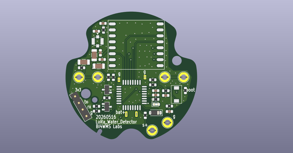
LoRa Flood Sensor Development Series - Part 3 PCB Placement Guide
LoRa Flood Sensor Development Series – PCB Placement Guide
Design Overview
We are using an existing enclosure for a shell-fit PCBA design.
- Enclosure outer diameter: 50mm
- Due to waterproof design, the internal space is quite limited.
- The other side must accommodate a coin cell battery, therefore only single-sided component placement is allowed.
Step 1: Determine PCBA Outline
- Locate the internal PCBA dimension drawing of the enclosure.
- Open the drawing with CAD software (AutoCAD, DraftSight, etc.).
- Carefully study the drawing and identify keep-out areas (regions where components are prohibited).
Step 2: Create Board Outline in KiCad
- Open your project in KiCad.
- Import the PCBA outline:
- Go to File → Import → Graphics (or use DXF import).
- Select the prepared dimension file and import it.
- After import, delete all unnecessary graphics and layers.
- Keep only the final PCBA board outline on the Edge.Cuts layer.
Step 3: Component Layout Guidelines
The layout is relatively simple due to single-sided constraints. Follow these rules:
- Single-sided component placement only.
- Place filtering capacitors as close as possible to the power pins of ICs.
- Arrange components following the signal flow direction.
- Position connectors, electrodes, and buttons exactly according to the mechanical drawing specifications.
- Pay special attention to height restrictions — check component height in limited clearance areas.
- Reserve enough space for the coin cell battery on the opposite side.
3D Effect Verification
After completing the layout and assigning 3D models in KiCad:
- Use View → 3D Viewer to check the overall assembly.
- Verify clearance with the enclosure and coin cell battery.
- Ensure no component interference with the waterproof shell.
Key Design Principles Summary
- Strictly follow mechanical constraints and keep-out zones
- Prioritize signal integrity and power integrity
- Place decoupling capacitors near power pins
- Maintain sufficient clearance for battery and waterproofing
- Pay attention to component height restrictions
- Optimize component placement according to signal flow
This post is licensed under CC BY 4.0 by the author.