KiCad Tutorial 2026: Useful Tools in PCB Design - Part 4
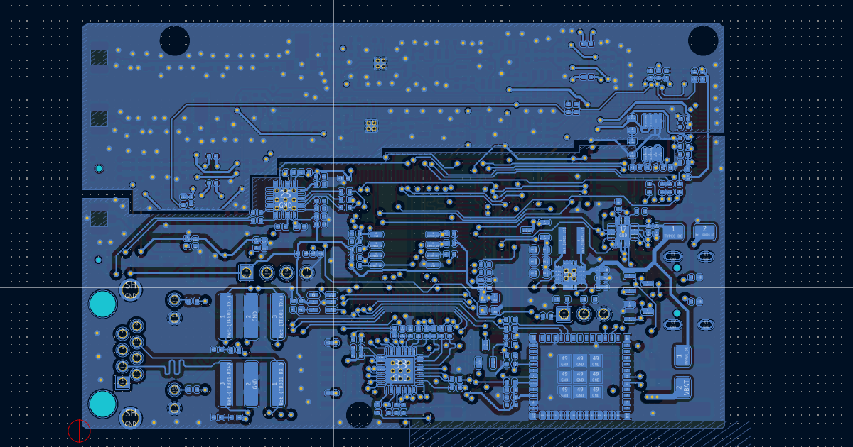
KiCad Tutorial 2026: Useful Tools in PCB Design - Part 4
KiCad Circuit Design Software Usage Guide
Part 4: Useful Tools in PCB Design
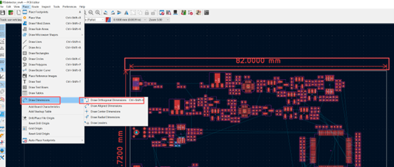
4.1 Add Dimension Annotations
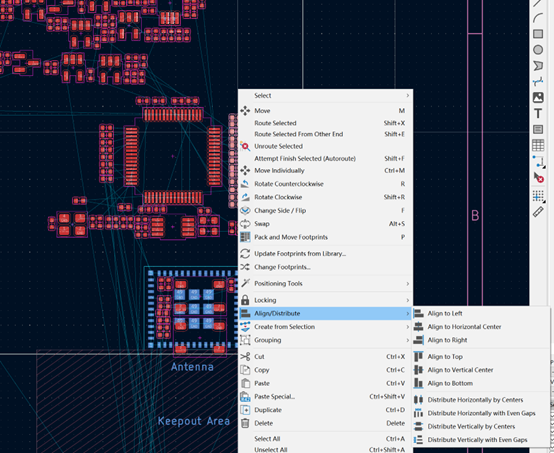
4.2 Align Components
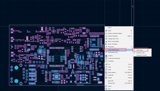
4.3 Chamfer Board Outline
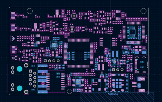
4.4 Show/Hide Net Connections

4.5 Hide Reference Designators in 3D View
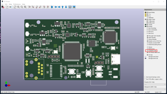
4.6 Define Routing Rules
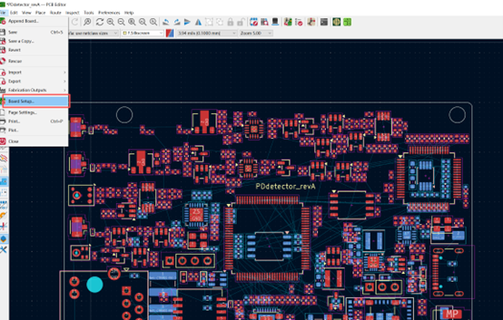
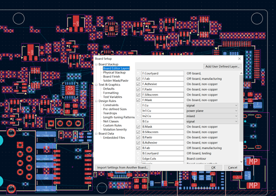
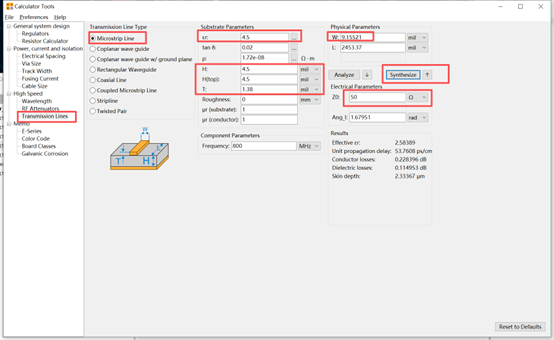
4.7 Set 50 Ohm Impedance Traces
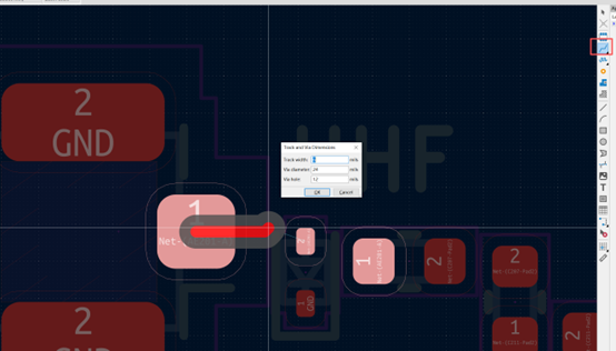
4.8 Adjust Trace Width During Routing,Shortcut key: “E”
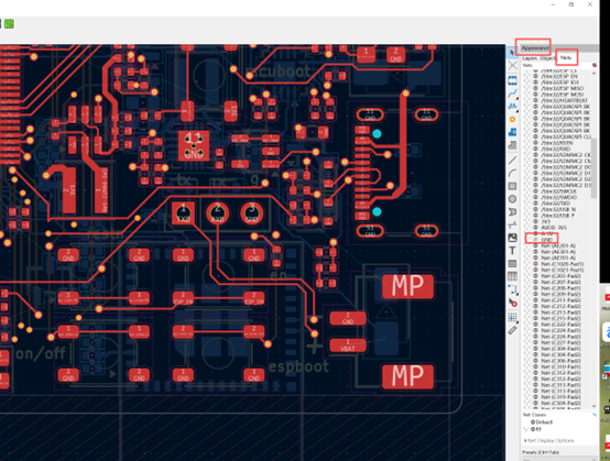
4.9 Hide Specific Net Ratsnest Lines
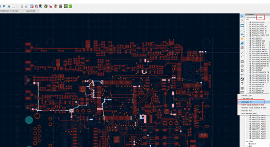
4.10 Highlight Nets
4.11 Hide Silkscreen Reference Designators
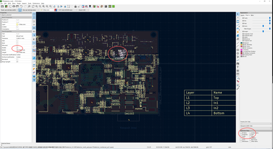
4.12 Length Matching Routing,Use the length tuning tool.
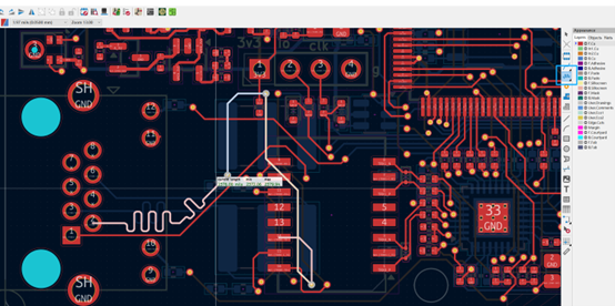
4.13 Batch Modify Via Sizes
- Select the region
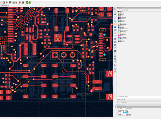
- Modify via parameters
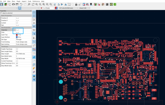
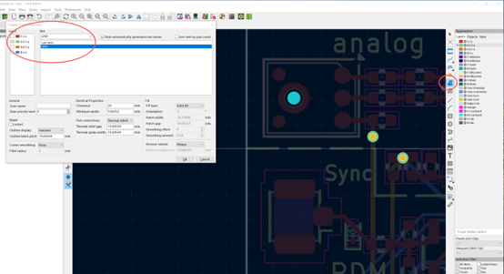
4.14 Set Copper Pour Nets
This post is licensed under CC BY 4.0 by the author.