KiCad Tutorial 2026: How to Use KiCad to design the schematic - Part 1
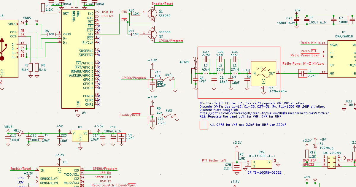
KiCad Tutorial 2026: How to Use KiCad to design the schematic - Part 1
KiCad Circuit Design Software Usage Guide
Part 1: Schematic Design step by step
1.1 Create a New Project
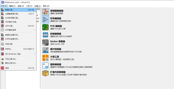
1.2 Open Schematic Design

1.3 Double-click to Open the Schematic
By default, this opens the root schematic page. 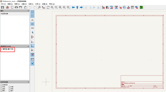
1.4 Use Hierarchical Schematic Structure
The root directory mainly defines the overall logical relationships. 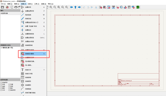
1.5 Create Hierarchical Schematics
Assign meaningful names to hierarchical schematic sheets. 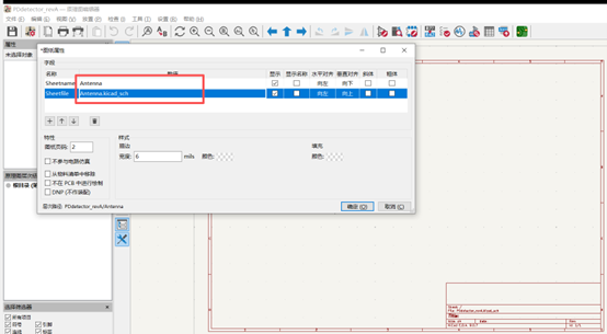
1.6 Enter Specific Sheets
Select components and begin drawing the schematic. 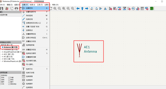
1.7 Configure Display Settings
Adjust page view, cursor, and display preferences. 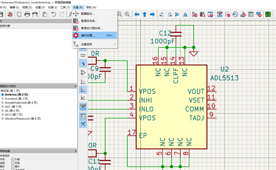
1.8 Draw Schematic Symbols
Use and modify existing symbols as needed. 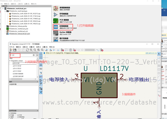
1.9 Create a Schematic Library
Manage custom schematic symbols efficiently. 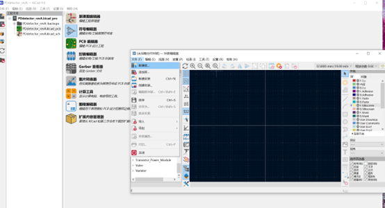
1.10 Save Symbols to Your Library
Store completed symbols in your custom library for reuse. 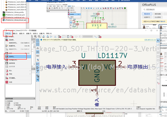
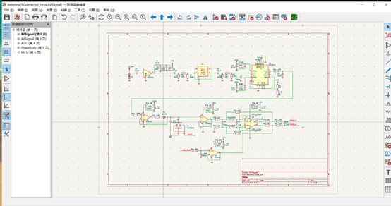
1.11 Complete the Schematic Framework
This post is licensed under CC BY 4.0 by the author.