SimpleFOC Integrated Board from Zero to One - Part 2
SimpleFOC Integrated Board Hardware Practice: From Zero to One (2) – From Schematic to PCB Layout, Teaching You How to Design an FOC Control Board That Can Be Directly Mounted on the Motor
This article explains the complete process of creating this SimpleFOC circuit board from scratch, along with all the detailed considerations in the hardware design.
Overall Design Considerations
The previous article mentioned some advantages and disadvantages of the official design. Combining those points, the following considerations were made:
- Solve the problem of separate driver and control boards with low integration by integrating the driver and control circuits onto a single board.
- Make it easy to mount directly on the rear of a brushless motor by using a circular board outline, which looks neat and coordinated when installed on the motor tail.
- When mounting on the motor tail, mechanical mounting holes must be included on the board to securely fix it to the motor. At the same time, the onboard magnetic encoder must be placed at the geometric center of the board, directly facing the motor’s magnetic ring, to enable closed-loop position control.
- Use the DRV8313 integrated MOSFET driver chip supported by the official SimpleFOC code to facilitate a compact design.
- Use the AS5600 magnetic encoder supported by the official code, while reserving ABZ encoder interfaces and I2C interfaces for easy expansion.
- Add low-side current sampling circuitry to enable closed-loop current control.
- Integrate a USB-to-serial chip on the board with a direct Type-C interface for convenient user debugging. A single Type-C data cable connects to the computer—no more hunting for USB-to-serial adapters. An additional TTL serial port is also reserved for easy integration into projects that need to control motors.
- For the user interface, add a heartbeat indicator LED to show the system operating status.
- Arduino has excellent support for the STM32 series microcontrollers, and STMicroelectronics officially supports Arduino as well. Considering the richer hardware resources of STM32 chips compared to ESP series (which are more consumer-oriented), the common STM32F103CBT6 was selected.
- For the power supply chip, Texas Instruments solutions offer excellent cost-performance. Two options were considered: TPS54302/TPS54202 or TPS5450D, differing mainly in output current and input voltage rating. To match the DRV8313, the higher voltage-rated TPS5450D was initially chosen. (Three versions were designed in total: the first two used TPS5450D; the final Rev C version switched to TPS54202 for smaller size, lower power, and easier hand-soldering DIY.)
These 10 considerations basically cover all the key details needed for the design.
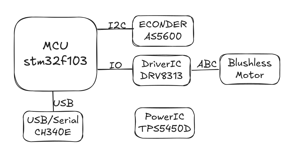
Overall Hardware Architecture Block Diagram
MCU + Driver + Power Supply + Magnetic Encoder + USB-to-Serial
Main Chip Selection Rationale
- Main controller: STM32F103CBT6
- Magnetic encoder: AS5600
- Driver chip: DRV8313
- Power supply chip: TPS5450D
These have already been explained in the design considerations above.
- USB-to-serial chip: For small size, the CH340 series CH340E in MSOP package was chosen. It requires no external crystal, making it highly suitable.
- Current-sense amplifier: The compact, cost-effective SGM8199A1XC6G was selected.
Schematic Design
The hardware was designed using Altium Designer. Source files are available for download on GitHub.
The schematic is relatively simple. Here’s a quick analysis:
Top-left section: STM32F103 minimum system circuit. Key points to note:
- The pins controlling the DRV8313 (IN1, IN2, IN3) must use timer channels.
- Current-sense inputs must use ADC pins.
- A switch was added to BOOT0 for convenient BOOT-mode programming.
This version is the Rev C schematic, which adds PWM receiver remote control and rotary knob speed control as reserved features.
Since the microcontroller itself supports USB CDC, the CH340E was designed with compatibility in mind, and it can be removed if desired.
Rev C Circuit Board Layout
A circular board design with a diameter of 43 mm was adopted. Four 3 mm elongated slots are cut in the center, compatible with 2204–4010 size brushless motors. These slots also naturally divide the board into functional zones, reducing interference: one zone for the microcontroller system, one for the switching power supply, and one for the driver circuit.
The front side contains the power indicator LED, system status LED, DRV driver chip, buttons, and interface components.
The back side holds most of the SMD components. Since JLCPCB’s SMT service is very affordable, all SMD parts were placed on one side. Only a few larger through-hole components that are easy to hand-solder are on the other side. The two indicator LEDs had to be placed on the back of the magnetic encoder chip because the encoder must face the motor tail directly.
Routing Instructions
Top Layer
Fewer components. Mainly power ground and high-current traces for the DRV driver chip, plus control lines. Control lines are guarded with ground to reduce interference.
Second Layer
Complete ground plane with strong/weak current area separation lines to maximize isolation between power and signal sections and minimize interference.
Third Layer
Used for sensitive traces, such as current sampling lines.
Bottom Layer
Most components are here. Routing follows the pre-planned regional divisions—each functional block stays within its own area. Differential pairs and sensitive signals are kept away from interference sources as much as possible.
Complete Design Materials
Reference: https://github.com/bi4wms/SimpleFOC
Next Article Preview:
In the next article, we will explain in detail how to quickly set up the SimpleFOC software and hardware environment (specifically for this integrated board).